

IanCanada
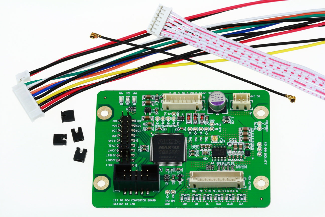
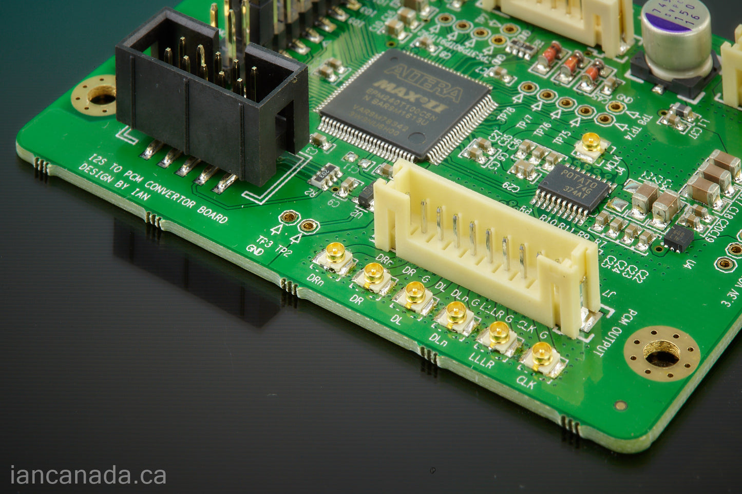
I2S to PCM converter board V2.0
I2S to PCM converter board V2.0
5.0 / 5.0
(8) 8 total reviews
Couldn't load pickup availability
Highly recommend the #9B PCM board with all 10 U.FL connectors pre-assembled. Manually assembling the U.FL connectors is not an easy job unless you are very skilled or have the professional tools. Unproperly soldering those connectors can result in project failure or affecting the sound quality.
Note:
The colors of a PH2.0 cable may not corresponding to the VCC(5V) and GND. Please be very very careful not to reverse VCC and GND wires of the PH2.0 connector that plugs to J6 . Otherwise the PCM board will be damaged and can not be fixed.
Descriptions
Many people still like the sound of traditional MULTIBIT audio DACs, such as AD1865/62, PCM1704/02, PCM63, TDA1541/A, and many others, because they convert digital music into analog in a different way than popular DELTA-SIGMA DACs.
However, most of those MULTIBIT DACs were designed having to work with digital filter chip through an interface we called "PCM", which transmits left and right data simultaneously. In this case, the problem would be that the sound quality and the maximum Fs of MULTIBIT DACs can be limited by the performance of the hardware based over sampling digital filter chip due to the low internal calculating accuracy, the resource saving interpolating algorithm, and the old higher jitter hardware technology.
In order to boost the sound quality by introducing low jitter technology and to play higher Fs music, we need to get rid of the limitation of that digital filter chip by driving the MULTIBIT DAC from higher performance software base real-time up-sampling filter or high Fs music stream directly. So, we need a jitter optimized device to run MULTIBIT DAC at NOS mode from an I2S bus.
This I2S to PCM converter board was developed exactly for this purpose under the requirement of audiophiles.
Features
- Support 16,18,20,24 bit PCM format output
- Accept 16 to 32bit I2S input signals with SCK from 32*Fs to 64*Fs
- Pure NOS mode with bit-perfect format converting
- High speed design capable for 384KHz Fs with maximum MCLK up to 100MHz
- Support PCM63,AD1865,AD1862,PCM1704,PCM1702,TDA1541/A and many other classical MULTIBIT DACs
- Support TDA1541/A working at offset binary mode
- Jumper selectable full-speed mode and half-speed mode
- L,R simultaneous timing, launching D/A conversion at same latching edge to eliminate L/R phase difference
- In order to reduce DAC noise floor, bit clock can be stopped after data shifted into DAC (default)
- Delayed falling edge of latch enable signal (LLLR) applied to stop clock mode
- Support dual mono DAC configuration
- Jitter optimized synchronize logic architecture with last stage high speed low noise re-clocking flip-flops driven by original MCLK
- With same physical dimensions, it can be assembled stacking on top of the FIFO clock board to save space
Documents
https://github.com/iancanada/DocumentDownload/tree/master/PCMboard
Share
Fast shipping, great porduct and very nice built. Thanks
Excellent product! The best always!!
Highly recommended - this little board works great! Two suggestions if you buy one:
1) install U.FL connectors and use U.FL cables to achive the best input and output signal.
2) double check the polarity of the power connection to the board, I have a sack of cables with PH2.0 connectors that seem to be standard on all other Ian Canada boards, except this board. The correct polarity is clearly labeled on the board, so it easy to check.
It is a good one, made my 1541A sounds amazing.
I used the PCM board to run my two Gapster TD1 DAC boards in balanced mode and it worked perfect.